Inline non-destructive 3D X-Ray inspection for SMT, DIP, and IGBT semiconductors — covering BGA, LGA, CSP, SOP, QFP, QFN, transistors, R/C-IGBT, bottom electrodes, power modules, POP, connectors, and THT components. High-speed dynamic imaging combined with multi-angle projection reconstruction reveals hidden defects no optical inspection can see.
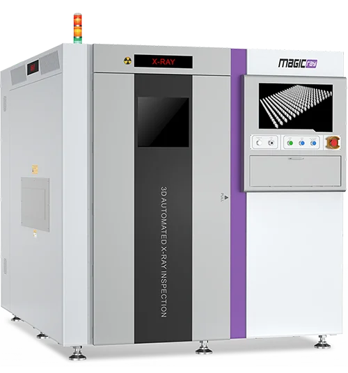
VX2000 uses high-speed dynamic imaging and circular multi-angle projection reconstruction technology to obtain complete volumetric data — enabling fully automatic inline X-Ray inspection of SMT, DIP, and semiconductor components.
Detection speed reaches 1.7 seconds per FOV — designed to keep up with high-throughput SMT lines without becoming the inspection bottleneck.
7 projection styles and 7 resolution types adapt to widely varying usage scenarios — from fast routine inspection to deep CT analysis of critical components.
Supports 3 separate programming styles with one-touch value-learning functionality — quick setup for new boards, no expert operator required.
The three-view interface makes diagnosing defects significantly more intuitive — engineers can pinpoint exactly where in the volume a defect occurs.
Dual linear motors with grating ruler feedback ensure precise, repeatable positioning at high speeds — accuracy you need for fine-pitch BGA analysis.
BGA, LGA, CSP, SOP, QFP, QFN, transistors, R/C-IGBT, bottom electrodes, power modules, POP, connectors, and THT components — one machine covers them all.
Hidden solder joints and dense fine-pitch packages are where X-ray inspection earns its place on the line — beyond what any optical AOI can see.

VX2000 inspects what AOI never reaches — solder joints hidden under packages, microvoids inside power modules, fractured vias deep in multilayer boards.
VX2000 combines proprietary 3D inspection algorithms aligned with IPC standards, flexible projection programming, 3D image analysis, and AI noise reduction — purpose-built for hidden-joint defects that no optical method can see.
Proprietary algorithms align directly with IPC standards — highly accurate inspection of BGA void rate and DIP pin fill-rate, the two most critical X-Ray inspection metrics.
7 projection styles and resolution types — trade off between image quality (6µm, 8µm for deep analysis) and inspection speed (25µm, 30µm for routine) on the same board.
Programming and maintenance stations both feature X-Y, Y-Z, and X-Z views — improves programming accuracy and provides intuitive defect diagnostics.
Three-dimensional images generated by 3D analysis enable intuitive, high-precision defect diagnosis — see exactly where a void sits inside a BGA ball.
Deep learning removes noise from low-dose images — faithful component reconstruction and accurate image data even at higher inspection speeds.
Multi-angle projection reconstruction produces up to 400 layers of CT data per board — depth resolution needed for stacked-die packages and multi-layer PCBs.
VX2000 is available as 3D AXI (standard) and XL 3D AXI (larger inspection envelope).
| Specification | 3D AXI | XL 3D AXI |
|---|---|---|
| Image System | ||
| 3D image reconstruction | Dynamic image capture + circular multi-angle projection reconstruction | |
| Resolution | 6, 8, 10, 15, 20, 25, 30µm | 8, 10, 15, 20, 25, 30µm |
| Number of 3D projections | 32, 48, 64, 128, 256, 512, 1024 | |
| X-Ray tube | Microfocus X-ray source | |
| X-Ray tube voltage / current | 30–130 kV, 10–300 µA | |
| X-Ray detector | CMOS flat panel detector | |
| Movement Structure | ||
| X/Y movement | Dual-drive linear motor with grating ruler feedback | |
| Platform | Granite | |
| Width adjustment | Automatic | |
| Board loading direction | Dual direction | |
| Board clamping | Automatic | |
| Hardware Configuration | ||
| Operating system | Windows 11 | |
| Communication | Ethernet, SMEMA | |
| Power requirement | Single phase 220V, 50/60Hz, 16A | |
| Air requirement | 0.5–0.6 MPa | |
| Conveyor height | 900 ± 20mm | |
| Equipment dimensions | L1730 × D2000 × H1715mm | L1835 × D2110 × H1715mm |
| Equipment weight | 3760 kg | 4280 kg |
| Radiation | Allowable leakage < 0.5 µSv/h | |
| PCB Handling | ||
| PCB size | 50 × 50 – 610 × 510mm | 100 × 50 – 750 × 610mm |
| Warping | ± 3mm | |
| PCB weight | ≤ 7 kg | ≤ 15 kg |
| Component clearance | Top 80mm · Bottom 40mm | |
| Clamping edge | 3.0mm | 4.0mm |
| Inspection Categories | ||
| Components | BGA, LGA, CSP, SOP, QFP, QFN, transistors, R/C-IGBT, bottom electrodes, power modules, POP, connectors, THT components, etc. | |
| Defects detected | Bubble, open solder, insufficient solder, solder volume, offset, bridging, solder climbing, THT solder fulfillment, solder bar, etc. | |
| Inspection Capabilities | ||
| Max. CT layers | 400 layers | |
| Max. speed | 1.7s / FOV | |
| Service & Support (NETA Trading) | ||
| US distributor | NETA Trading LLC · Lake Bluff, IL | |
| Installation & training | On-site installation, commissioning, and operator training | |
| Live demo | Lake Bluff, IL · Remote demo available — subject to current equipment availability in the demo center. | |
Configuration and specifications subject to change — contact us to confirm for your line.
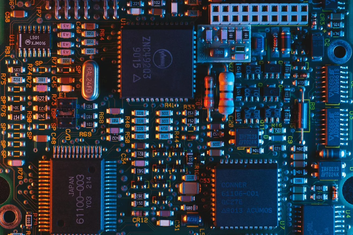
X-Ray inspection sees what optical can't — hidden solder joints under BGAs, voids inside power modules, broken vias deep in multilayer PCBs. VX2000 is the post-reflow gatekeeper for the defects nobody else catches.
Voids, opens, shorts, and bridging under BGAs, LGAs, and CSPs — failures invisible to AOI but the leading cause of board returns.
Solder voiding in IGBT and power module substrates — thermal reliability of EV inverters, solar invertors, and industrial drives depends on it.
Pin fill-rate inspection on through-hole connectors and DIPs — IPC-compliant verification of solder climbing and joint integrity.
PoP, flip-chip, and 2.5D/3D advanced packages — VX2000's 400-layer CT capability resolves stacked-die defects nothing else can image.
Tell us about your line and the defects you're hunting — we'll help you choose between VX2000 3D AXI and XL based on your board sizes and inspection depth.